Engineering (PCBA) Printed Circuit Board Assembly for modern electronics devices has become both simple and advanced at the same time.
It has become simple, as modern devices focus more and more on integrating various functions onto one chip (System on Chip or SoCs). Thus simplifying engineering PCBA design. This is true for smaller devices such as tablets, phones and smart watches. Complexity comes from larger, and more advanced machines, especially prototypes or first releases that have yet to employ the integration of some components in order to create proofs-of-concept. Other factors also come into play in the engineering PCBA for modern electronics devices.
Size of Devices
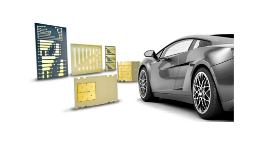
The increasingly shrinking devices such as smartwatches and phones have presented quite a challenge for the engineering PCBA. The increase of production of such devices as well as new form factors like Apple’s Trashcan and the new Mac Pro and IoT devices have forced PCB makers to find new materials and come up with new techniques to create flexible and high-density solutions. The newer trend now is the creation of voltage and high-temp resistant PCBs for the influx of electric vehicles. These are made on the larger scale and should be made more tolerant to higher voltages and temperature.
Materials
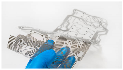
Because of the continually shrinking electronics, such as wearables and anorexic phones and laptops, engineers need to look into using other unconventional materials to produce more flexible and possibly stretchable PCBs. Lightweight flexible PCBs have been in use for a while now. They have contributed greatly to reduce weight and costs of electronics.
The greatest challenge engineers have when it comes to materials to the compliance to the Restriction of Hazardous Substances Directive (RoHS) that continuously aims to wean the electronics industry away from traditional but harmful substances such as lead and mercury. This makes more sense as e-waste continues to accumulate worldwide thanks to the increasing demand for, and disposal of consumer electronics.
AR/VR
It is currently being used by some PCB makers in designing and building new PCBs. AR and VR are becoming handy in training and guiding personnel. This is thanks to heads up displays that contain the necessary guides and instructions needed. All without having to flip through manuals. They’re also now very handy in diagnostics, maintenance and repair.
3D Printing
Thanks to 3D printing, a new avenue has opened up for Printed Circuit Board Assembly (PCBA). MIT’s Computer Science and Artificial Intelligence Laboratory (CSAIL) managed to make it a reality by managing to print substrates, components and processing circuitry. The technology needs a little time to mature. But this should make possible the ability to engineer PCBs in all shapes and sizes and possibly make simple PCB manufacturing much more affordable.

Security
Incorporating security right into the PCB itself didn’t used to be the concern of PCB makers. This is because it was the realm of the chipmakers and software engineers. But recent security breaches that directly hack into hardware such as the Meltdown, Spectre, the baby monitor scare, and now infra-red hacking of IoT devices, necessitates the need for PCB manufacturers to chip in security measures built-into PCBs. Much like unique MAC addresses on NICs, IBM researchers are trying to find ways to embed cryptographic keys directly into PCB substrates. For PCB makers that include other electronic components into their Printed Circuit Board Assembly (PCBA), MIT has already found ways of embedding these keys into silicon. These keys will actually be accessible and not just etched initials of the engineers.
Safety and Productivity
And lastly, electrostatic discharge remains an issue during assembly of Printed Circuit Board Assembly and manufacture of semiconductors. Thankfully, modern PCBs assembly has it better with built-in ESD protection in assembly lines and working tables.