Giltronics Associates Inc.a leader in the PCB product industry. We are not only a manufacturer but also an innovator in PCB industry. We have invented sophisticated processes and constructed advanced facilities for our PCB development. We have designed and produced many different types of PCB products including rigid PCB, flexible PCB, and rigid-flex printed circuit boards. We also provide OEM turnkey services and solutions.
Giltronics Associates Inc. focuses on the development of multi-layer boards characterized with high density IVH substrates, microvia, fine pattern, and extra thin layers. We are committed to providing superior products are in compliance with the following rigorous industry standards: QS 9000, ISO 9001, ISO 9002, ISO 14001, UL recognition.
How do you reduce your Printed Circuit Board (PCB) cost and streamlined manufacturing process?
Giltronics offers many different types of printed circuit boards that will fit your design. We offer single sided, double sided, multi-layers, and rigid –flex Circuits. The PCB serves as a convent interconnect and is widely used in today electronics. The Flex circuit will enable you to put a complex circuit in a small space or give it the flexibility into areas a rigid PCB won’t fit.
In the Aero space industry weight is a big factor and the flex circuit fits this application head on with Polyimide materials 1 mil thickness very light weight. In the auto industry – interconnects throughout the dash board connecting electronics to, LED lighting, LED tail lights and seat heating elements. Other applications are Aero space, Medical Electronics, Audio- electronics and Industrial electronics. Giltronics has the solution for your design.
The PCB materials are all certified to UL standards and are inspected as it enters the plant. Materials CEM-1, CEM-3, FR-4, Rogers, Aluminum, Kapton, Polyimide, Polyester are widely used by our customers.
A printed circuit board, or PCB, is used to mechanically support and electrically connect electronic components using conductive pathways, tracks or signal traces etched from copper sheets laminated onto a non-conductive substrate. When the board has only copper tracks and features, and no circuit elements such as capacitors, resistors or active devices have been manufactured into the actual substrate of the board, it is more correctly referred to as printed wiring board (PWB) or etched wiring board. Use of the term PWB or printed wiring board although more accurate and distinct from what would be known as a true printed circuit board, has generally fallen by the wayside for many people as the distinction between circuit and wiring has become blurred. Today printed wiring (circuit) boards are used in virtually all but the simplest commercially produced electronic devices, and allow fully automated assembly processes that were not possible or practical in earlier era tag type circuit assembly processes.
Patterning (etching)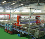 The majority of printed circuit boards today are made from purchased laminate material with copper already applied to both sides. The unwanted copper is removed by various methods leaving only the desired copper traces, this is called subtractive. In an additive method, traces are electroplated onto a bare substrate using a complex process with many steps. The advantage of the additive method is less pollution of the environment. The method chosen for PCB manufacture depends on the desired number of boards to be produced. Double-sided boards or multi-layer boards use plated-through holes, called vias, to connect traces on different layers of the PWB.
Additive processes
Additive processes adds desired copper traces to an insulating substrate. In the full additive process the bare laminate is covered with a photosensitive film which is imaged (exposed to light though a mask and then developed which removes the unexposed film). The exposed areas are sensitized in a chemical bath, usually containing palladium and similar to that used for through hole plating which makes the exposed area capable of bonding metal ions. The laminate is then plated with copper in the sensitized areas. When the mask is stripped, you have a finished PCB.
The most common is the “semi-additive” process: the unpatterned board has a thin layer of copper already on it. A reverse mask is then applied. (Unlike a subtractive process mask, this mask exposes those parts of the substrate that will eventually become the traces.) Additional copper is then plated onto the board in the unmasked areas; copper may be plated to any desired weight. Tin-lead or other surface platings are then applied. The mask is stripped away and a brief etching step removes the now-exposed bare original copper laminate from the board, isolating the individual traces. Some single-sided boards which have plated-through holes are made in this way. General Electric made consumer radio sets in the late 1960s using additive boards. In 1977 Dr.J.F.Mansfeld (N.V. Philips Gloeilampenfabrieken) presented the PD-R process (Physical Development by Reduction) in a speech at the Hotel International Zurich.[citation needed]
The additive process is commonly used for multi-layer boards as it facilitates the plating-through of the holes to produce conductive vias in the circuit board.
Circuit properties of the PCB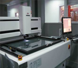 Each trace consists of a flat, narrow part of the copper foil that remains after etching. The resistance, determined by width and thickness, of the traces must be sufficiently low for the current the conductor will carry. Power and ground traces may need to be wider than signal traces. In a multi-layer board one entire layer may be mostly solid copper to act as a ground plane for shielding and power return. For microwave circuits, transmission lines can be laid out in the form of stripline and microstrip with carefully controlled dimensions to assure a consistent impedance. In radio-frequency and fast switching circuits the inductance and capacitance of the printed circuit board conductors become significant circuit elements, usually undesired; but they can be used as a deliberate part of the circuit design, obviating the need for additional discrete components.
Chemical etching
Chemical etching is usually done with ammonium persulfate or ferric chloride. For PTH (plated-through holes), additional steps of electroless deposition are done after the holes are drilled, then copper is electroplated to build up the thickness, the boards are screened, and plated with tin/lead. The tin/lead becomes the resist leaving the bare copper to be etched away.
The simplest method, used for small-scale production and often by hobbyists, is immersion etching, in which the board is submerged in etching solution such as ferric chloride. Compared with methods used for mass production, the etching time is long. Heat and agitation can be applied to the bath to speed the etching rate. In bubble etching, air is passed through the etchant bath to agitate the solution and speed up etching. Splash etching uses a motor-driven paddle to splash boards with etchant; the process has become commercially obsolete since it is not as fast as spray etching. In spray etching, the etchant solution is distributed over the boards by nozzles, and recirculated by pumps. Adjustment of the nozzle pattern, flow rate, temperature, and etchant composition gives predictable control of etching rates and high production rates.
As more copper is consumed from the boards, the etchant becomes saturated and less effective; different etchants have different capacities for copper, with some as high as 150 grams of copper per litre of solution. In commercial use, etchants can be regenerated to restore their activity, and the dissolved copper recovered and sold. Small-scale etching requires attention to disposal of used etchant, which is corrosive and toxic due to its metal content.
The etchant removes copper on all surfaces exposed by the resist. “Undercut” occurs when etchant attacks the thin edge of copper under the resist; this can reduce conductor widths and cause open-circuits. Careful control of etch time is required to prevent undercut. Where metallic plating is used as a resist, it can “overhang” which can cause short-circuits between adjacent traces when closely spaced. Overhang can be removed by wire-brushing the board after etching.
Lamination
“Multi layer” printed circuit boards have trace layers inside the board. One way to make a 4-layer PCB is to use a two-sided copper-clad laminate, etch the circuitry on both sides, then laminate to the top and bottom prepreg and copper foil. Lamination is done by placing the stack of materials in a press and applying pressure and heat for a period of time. This results in an inseparable one piece product. It is then drilled, plated, and etched again to get traces on top and bottom layers. Finally the PCB is covered with solder mask, marking legend, and a surface finish may be applied. Multi-layer PCB’s allow for much higher component density.
Drilling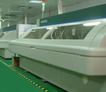 Holes through a PCB are typically drilled with small-diameter drill bits made of solid coated tungsten carbide. Coated tungsten carbide is recommended since many board materials are very abrasive and drilling must be high RPM and high feed to be cost effective. Drill bits must also remain sharp so as not to mar or tear the traces. Drilling with high-speed-steel is simply not feasible since the drill bits will dull quickly and thus tear the copper and ruin the boards. The drilling is performed by automated drilling machines with placement controlled by a drill tape or drill file. These computer-generated files are also called numerically controlled drill (NCD) files or “Excellon files”. The drill file describes the location and size of each drilled hole. These holes are often filled with annular rings (hollow rivets) to create vias. Vias allow the electrical and thermal connection of conductors on opposite sides of the PCB.
When very small vias are required, drilling with mechanical bits is costly because of high rates of wear and breakage. In this case, the vias may be evaporated by lasers. Laser-drilled vias typically have an inferior surface finish inside the hole. These holes are called micro vias.
It is also possible with controlled-depth drilling, laser drilling, or by pre-drilling the individual sheets of the PCB before lamination, to produce holes that connect only some of the copper layers, rather than passing through the entire board. These holes are called blind vias when they connect an internal copper layer to an outer layer, or buried vias when they connect two or more internal copper layers and no outer layers.
The hole walls for boards with 2 or more layers can be made conductive and then electroplated with copper to form plated-through holes. These holes electrically connect the conducting layers of the PCB. For multilayer boards, those with 3 layers or more, drilling typically produces a smear of the high temperature decomposition products of bonding agent in the laminate system. Before the holes can be plated through, this smear must be removed by a chemical de-smear process, or by plasma-etch. The de-smear process ensures that a good connection is made to the copper layers when the hole is plated through. On high reliability boards a process called etch-back is performed chemically with a potassium permanganate based etchant or plasma. The etch-back removes resin and the glass fibers so that the copper layers extend into the hole and as the hole is plated become integral with the deposited copper.
Exposed conductor plating and coating
PCBs are plated with solder, tin, or gold over nickel as a resist for etching away the unneeded underlying copper.
After PCBs are etched and then rinsed with water, the soldermask is applied, and then any exposed copper is coated with solder, nickel/gold, or some other anti-corrosion coating.
Matte solder is usually fused to provide a better bonding surface or stripped to bare copper. Treatments, such as benzimidazolethiol, prevent surface oxidation of bare copper. The places to which components will be mounted are typically plated, because untreated bare copper oxidizes quickly, and therefore is not readily solderable. Traditionally, any exposed copper was coated with solder by hot air solder levelling (HASL). The HASL finish prevents oxidation from the underlying copper, thereby guaranteeing a solderable surface. This solder was a tin-lead alloy, however new solder compounds are now used to achieve compliance with the RoHS directive in the EU and US, which restricts the use of lead. One of these lead-free compounds is SN100CL, made up of 99.3% tin, 0.7% copper, 0.05% nickel, and a nominal of 60ppm germanium.
It is important to use solder compatible with both the PCB and the parts used. An example is Ball Grid Array (BGA) using tin-lead solder balls for connections losing their balls on bare copper traces or using lead-free solder paste.
Other platings used are OSP (organic surface protectant), immersion silver (IAg), immersion tin, electroless nickel with immersion gold coating (ENIG), and direct gold plating (over nickel). Edge connectors, placed along one edge of some boards, are often nickel plated then gold plated. Another coating consideration is rapid diffusion of coating metal into Tin solder. Tin forms intermetallics such as Cu5Sn6 and Ag3Cu that dissolve into the Tin liquidus or solidus(@50C), stripping surface coating or leaving voids.
Electrochemical migration (ECM) is the growth of conductive metal filaments on or in a printed circuit board (PCB) under the influence of a DC voltage bias.Silver, zinc, and aluminum are known to grow whiskers under the influence of an electric field. Silver also grows conducting surface paths in the presence of halide and other ions, making it a poor choice for electronics use. Tin will grow “whiskers” due to tension in the plated surface. Tin-Lead or Solder plating also grows whiskers, only reduced by the percentage Tin replaced. Reflow to melt solder or tin plate to relieve surface stress lowers whisker incidence. Another coating issue is tin pest, the transformation of tin to a powdery allotrope at low temperature.
Solder resist
Areas that should not be soldered may be covered with “solder resist” (solder mask). One of the most common solder resists used today is called LPI (liquid photoimageable).[20] A photo sensitive coating is applied to the surface of the PWB, then exposed to light through the solder mask image film, and finally developed where the unexposed areas are washed away. Dry film solder mask is similar to the dry film used to image the PWB for plating or etching. After being laminated to the PWB surface it is imaged and develop as LPI. Once common but no longer commonly used because of its low accuracy and resolution is to screen print epoxy ink. Solder resist also provides protection from the environment.
Silkscreen
Line art and text may be printed onto the outer surfaces of a PCB usually by screen printing epoxy ink in a contrasting color, but can also be done with LPI or dry film like the solder resist. When space permits, the legend can indicate component designators, switch setting requirements, test points, and other features helpful in assembling, testing, and servicing the circuit board.
Some digital printing solutions are used instead of screen printing. This technology allows printing variable data onto the PCB, including individual serial numbers as text and bar code.
Test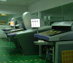 Unpopulated boards may be subjected to a bare-board test where each circuit connection (as defined in a netlist) is verified as correct on the finished board. For high-volume production, a bed of nails tester, a fixture or a rigid needle adapter is used to make contact with copper lands or holes on one or both sides of the board to facilitate testing. A computer will instruct the electrical test unit to apply a small voltage to each contact point on the bed-of-nails as required, and verify that such voltage appears at other appropriate contact points. A “short” on a board would be a connection where there should not be one; an “open” is between two points that should be connected but are not. For small- or medium-volume boards, flying probe and flying-grid testers use moving test heads to make contact with the copper/silver/gold/solder lands or holes to verify the electrical connectivity of the board under test. Another method for testing is industrial CT scanning, which can generate a 3D rendering of the board along with 2D image slices and can show details such a soldered paths and connections.